GaNonCMOS results – Testing
GaNonCMOS results brief 4
Today, in the fourth instalment of the GaNonCMOS results brief, we are looking into the key testing results that were achieved during the project.
Testing
An extensive test in industrial conditions, including both electrical and reliability tests, of the demonstrators and materials developed and fabricated throughout the project was performed.
Embedded magnetic sheet materials in different configurations –as a transformer or as an inductor with three gap options (no gap, 1 gap or 3 gaps inductors) – were fabricated (AT&S AG) and tested (RECOM). The inductance was selected as a main parameter and the influence of various environmental tests and production processes on the inductance and mechanical properties was analysed. The effect of these configurations on the inductance along with the temperature dependency and bias current was investigated using a customized semi-automated test system developed for this purpose (Figure 19).
Moreover, 50 panels with 33 samples on each panel of the embedded transformer were manufactured (AT&S AG). 10 different magnetic materials were used (5 panels each material). A customized fully-automated test setup was developed to be able to measure, record and process the primary and leakage inductance of each transformer sample of the panel (Figure 20). 5 types of environmental tests were performed (RECOM, AT&S AG) for each material:
- HST 1000h – 1000 hours High Temperature Storage at + 125°C
- LST 1000h – 1000 hours Low Temperature Storage at -55°C
- THB 1000h – Temperature Humidity Bias at 85°C/85%RH
- TCy – Temperature Cycling, 2000 cycles (-55°C to +125°C)
- HAST – Highly Accelerated Stress Test – 96 hours at 130°C, 85%RH, performed two times
All the panels went through a drying step and three times reflow before the environmental test started. These long-term tests were one to two times interrupted to perform the intermediate inductance measurements and visual check to assess the effect of any sudden change of the parameters.
An isolation test using hipot was performed on selected samples of each panel. Based on these measurements the current design is capable of at least 1kV.
All the panels were x-rayed before the environmental tests started to check if the material was not damaged during the embedding process (high pressure).
As a result, we were able to determine which materials out of these 10 tested were suitable for embedding. With the toroidal design with 10.5 mm diameter it is possible to reach inductance of about 1.6 uH using a magnetic material suitable for up to 2-3 MHz and currents up to 2-3 A. Other suitable material can go to about 10 MHz with the inductance up to 350 nH.
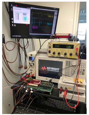
Figure 19: Semi-automated test setup for inductance measurements in temperature with bias current.
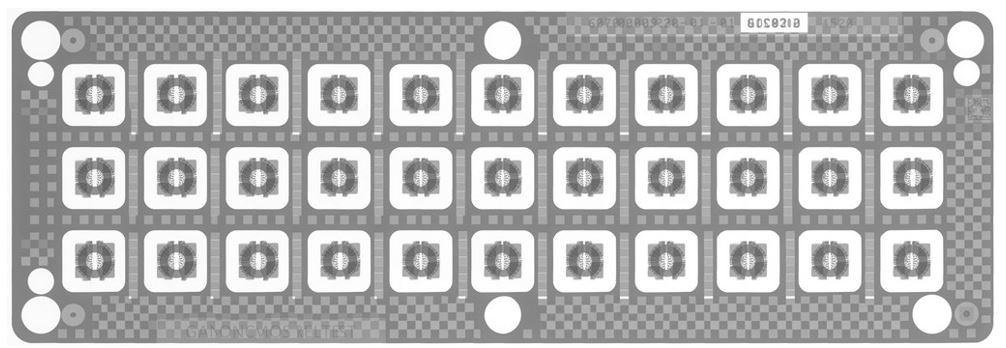
Figure 20: X-ray of the test panel
The DC/DC converter with embedded inductors (PCB DEMO 6) was also tested (Figure 21) by means of electrical tests (line and load regulation, ripple and efficiency) as well as environmental reliability tests (HTHH – 96 hours moisture test, HALT test and EMC measurements).
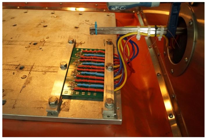
Figure 21: HALT test board with 4x PCB DEMO 6 in the chamber installed on the vibration pad.
Our complete results brief is also available for download here.