GaNonCMOS results – systems
GaNonCMOS results brief 3
Today follows the third instalment of our results brief, this time covering the results at system-level.
Systems
The GaNonCMOS project aims to bring GaN power electronic systems to the next level of maturity by providing the most densely integrated systems to date.
Advancements in the chip level demonstrators
An innovative step considered in the project is to integrate GaN power switches with CMOS drivers (Figure 10), being wafer-wafer bonding – a key technology to enable high frequency chip-scale demonstrators.
Throughout the project, the progress realized on the wafer bonding included the development of a suitable planarization technology (IHP GmbH) to achieve bonding-ready wafers. An optimized version of the combined controller/driver chip was adapted to meet the requirements for direct wafer bonding (IBM Research, Zurich) in the chip level demonstrator. At the same time, a double direct wafer bonding process for the co-integration of GaN devices and CMOS was designed (Figure 11). A process to perform aligned wafer bonding on two processed wafers was realized, and the first demonstration of this process was applied to integrate GaN epitaxial layers on silicon without change of polarity.
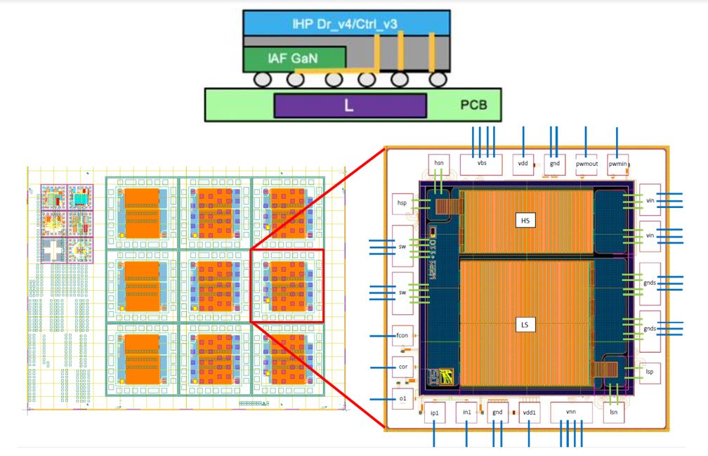
Figure 10: Highly integrated CMOS/GaN power switch.
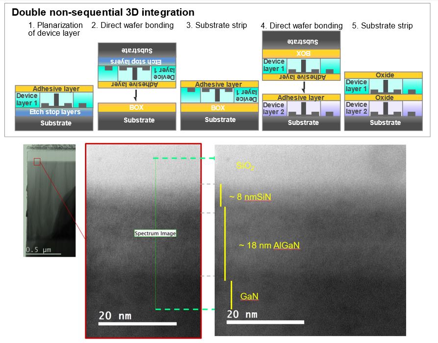
Figure 11: Double direct wafer bonding process for the co-integration of GaN devices and CMOS (top), EDS at the top SiO2/III-V interface (bottom).
Advancements in the package/stack level demonstrators
The GaN-based monolithically integrated half-bridge wire bonded chip or embedded chip was used in demonstrators (Fraunhofer IAF) to evaluate the quality and the performance of our design and fabrication as well as the efficiency of the embedding technology (AT&S AG):
- As first demonstrator, a wire bonded GaN/Si half-bridge switch has been used in a complete IAF-designed PoL (Point of Load) buck converter. The converter yields a system efficiency that approaches 82% at 2 A (for the half bridge alone), and 78% at 2 A (for the GaN switch + gate driver), when switching at 1 MHz and converting from 24 V to 1 V and from 12 V to 1 V (Figure 12).
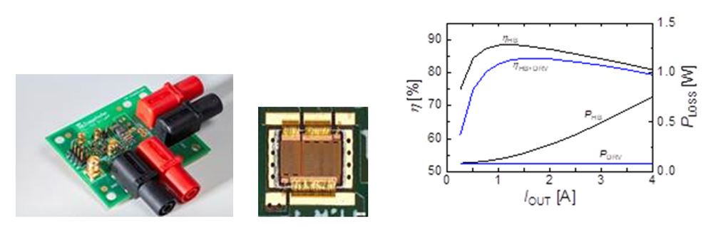
Figure 12: Performance of the bonded GaN PoL demonstrator (12 V-1V PoL).
- The second designed PoL buck demonstrator included an embedded monolithically integrated GaN chip associated to an embedded inductor chip. The performance of the buck converter is presented in Figure 13.
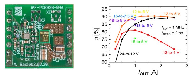
Figure 13: Embedded chip D5 (left), performance of the embedded PoL demonstrator (right).
The heterogeneous integration of the GaN HEMT switch (Fraunhofer IAF) and CMOS driver-controller (IHP GmbH), thin film magnetic materials (Tyndall) and advanced substrate embedding technologies (AT&S AG) is being considered for 12–48V Server Power Supply applications (IBM Research, Zurich), and Automotive (48V) and Aerospace (24V) products at RECOM, Austria.
The proof-of-concept voltage regulator (VR) prototypes by Tyndall focus on 12V “Buck” PoL converters employing the IAF 25V GaN HEMT switches (see Figure 14) and 48V LLC resonant converters employing 100V GaN HEMT switches. The LLC resonant has been used as a test-bed for new gate-driver ICs (Tyndall) employing MoS signal isolation and PCB embedded transformer with leakage resonant inductor. Throughout the project several modules were developed to implement a variety of topologies such as basic buck, 3-level buck and coupled inductor 2-phase modules. The basic buck is for in-converter evaluation of the controller, drivers and switching bridge, while the 3-level buck and the coupled-inductor 2-phase buck are to reduce the inductance value requirement and enable higher density integration
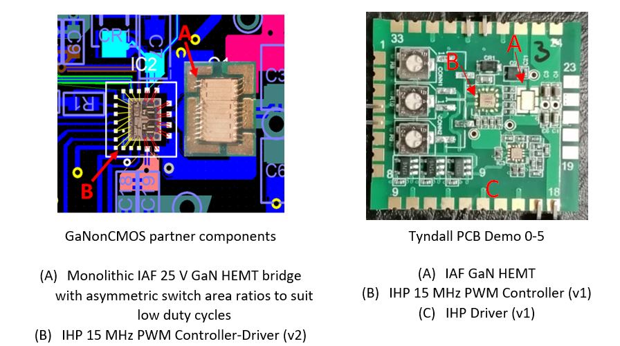
Figure 14: 2–10 MHz, 12 V Point-of-Load (PoL) Converter Modules – PCB-DEMO-5.
The “PCB-DEMO-5” test-bed has been used to characterize the in-converter performance of the new IAF and IHP magnetic components, individually, as well as collectively in a full closed loop system. The controller (v1), operates to 15 MHz (versus commercial PWM ICs which operate to about 2 MHz) and has a quiescent current draw, IQ, of 680 µA. The challenges identified include achieving better control performance for duty cycles in the range 0–10% at the higher frequencies. Regarding the closed-loop converter, although we are at early stages, we have full functionality. The 25 V GaN d-HEMT switches are performing as expected (Figure 15).
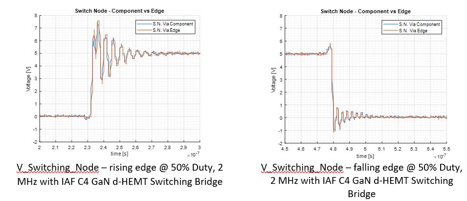
Figure 15: Performance of the 25 V GaN d-HEMT switches.
A full DC/DC converter (see Figure 16 and Figure 17) with embedded material in the inner layers of the PCB was also designed, developed and produced (RECOM, AT&S AG). This converter integrates the inductor in the PCB under a commercial LDMOS monolithic PMIC switcher. It is a functional demonstrator with a buried inductor based on a single IC solution. The single IC with silicon MOSFETs used is the same as in a standard RECOM power module, which allows the benchmark. The assembled DC/DC convertor demonstrates the embedded inductor technology in a real-like full-feature non-isolated converter. The main advantage here is a flat design – height reduction.
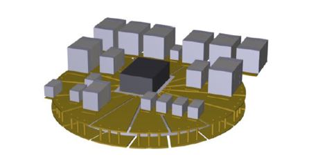
Figure 16: Components of the DC/DC converter designed by RECOM and AT&S.
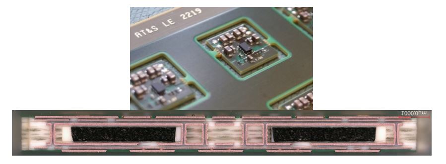
Figure 17: Assembled DC-DC converter and cross-section of PCB.
Spin-off system product development
A wireless charging unit was also developed and produced with the embedded inductor technology (AT&S AG). The wireless charging unit was constructed to prove that big inlays of magnetic material could be embedded in a PCB. With the working demonstrator it was possible to charge commercial phones and wireless earplugs.
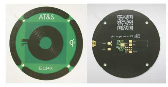
Figure 18: Wireless charging unit front and back side.
Our complete results brief is also available for download here.