GaNonCMOS results – materials
GaNonCMOS results brief 1
In the past week, the GaNOnCMOS consortium prepared a Results Brief on the key results achieved during the project period. It covers our main results in the areas of materials, components, system, testing and business and an outlook on the activities that will continue after the formal end of the GaNonCMOS project.
Today we’re starting with the key results on materials. In the coming days, the subsequent instalments will follow.
Materials
Throughout the GaNonCMOS project, the epitaxy of GaN on silicon substrates was developed and fine-tuned towards the fabrication of 25 V class devices based on GaN/AlGaN HEMT. The development, which relied on an optimized single transistor layout and standard process technology, revealed that the inclusion of an in-situ SiN passivation layer enabled the reduction of the leakage current also for large area switches. In addition, magnesium nitride thin films were alternatively explored as gate dielectric material for these devices. A series of Mg3N2 films grown by MBE on Si(100) and Si(111) substrates were investigated. In situ RHEED and ex situ XRD experiments reveal that polycrystalline Mg3N2 films are successfully grown when using moderate sample temperatures during MBE deposition. Remarkably, the Mg3N2 films appear to degrade very rapidly when exposed to ambient conditions. An in situ grown capping layer such as Mg, for example, forms an effective protection for the Mg3N2 films in ambient.
Aiming at the fabrication of integrated magnetic devices, the project also explored new magnetic core materials based on magnetic microparticles and thin films. Laminated thin films of a cobalt based amorphous alloy (CoZrTa or CZT) were optimised for use as the magnetic core material for integrated magnetic devices on-silicon or in-substrate. The permeability of this material remains stable up to 100 MHz. In parallel, anisotropic composite core materials for an inductor-based fully integrated voltage regulator were also investigated (see Figure 1 and Figure 2). The main findings out of the fabrication and characterization of composite magnetic materials were:
- The most effective composite assembly consists of a mixture of nano- and micro-particles.
- There is an enhancement of the magnetic properties by both the anisotropic structure and the “necking”.
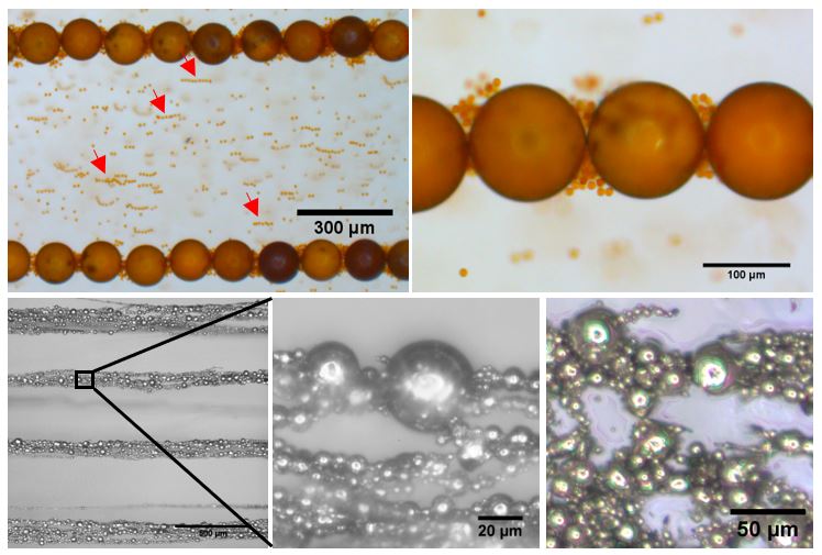
Figure 1: Optical microscope images of a magnetic composite assembly of nano- and micro-particles.
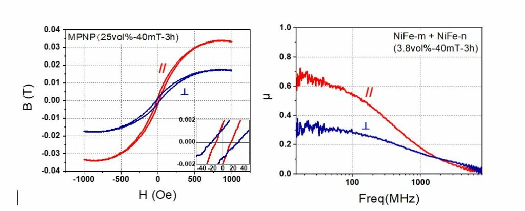
Figure 2: B-H characteristics and permeability versus frequency for composite assemblies.
In terms of characterization and reliability, a wide variety of commercial magnetic sheet materials, potentially suitable for PCB embedding were extensively evaluated for demonstrators and reliability properties. We learned that the CTE mismatch between the magnetic and the surrounding material should be as low as possible to avoid delamination (see Figure 3).
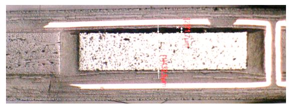
Figure 3: Delamination of embedded inlay.
For the reliability testing and evaluation of those embedded materials, a test array was designed and produced with 10 promising candidate magnetic materials (see “Testing”).
Thermal simulations of embedded inductors and complete board systems were conducted. The simulations carried out for the PCB demo 5 resulted in a maximum temperature below 40 °C, implying no anticipated thermal issues even though we are embedding very thin magnetic laminates (see Figure 4).
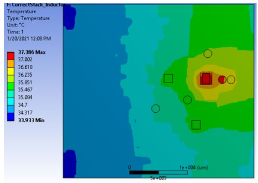
Figure 4: Thermal simulation of PCB demonstrator 5 board
Our complete results brief is also available for download here.