GaNonCMOS results – components
GaNonCMOS results brief 2
Today, we are presenting the second instalment of our results brief, this time focussing on the key component development achieved by the GaNOnCMOS project.
Components
In order to develop demonstrators, the partners have been working to manufacture and qualify the different components needed. The following components have been developed.
Controller and driver ICs
IHP worked on separate controller and driver circuits, which were designed for the evaluations of the key circuit blocks and achieved a measured efficiency of up to 94% in a PCB demonstrator together with IAF‘s GaN switches. Finally 2 versions of a combined controller/driver IC were developed:
- Half-bridge driver with general purpose PWM controller with minimum die size and extended features compared to the single chips (V1) (see Figure 5). The 1.5 x 1.8 mm² sized chip consumes only 30 mW working at 2 MHz PWM frequency and is able to deliver a driver peak output current of 1.8 A at both the low-side and high-side outputs.
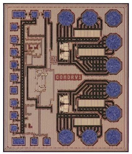
Figure 5: Photo of the combined driver/controller IC V1
- Half-bridge driver for GaN switches with general purpose PWM controller adapted for chip level demonstrator with direct wafer bonding (V2).
In addition, a 48 V driver output stage was produced in order to show the capability of IHP’s BiCMOS technology to be prepared for DC-DC converters with isolation voltages higher than 64 V.
GaN switches
At IAF different GaN switches were designed and fabricated based on the HEMTs technology, having a small chip size, a low on-state resistance, a high maximal available current (20 A or 40 A) and a breakdown voltage of 25 V or 100 V. Half-bridge converters were delivered by IAF to the other project partners for use in demonstrators as a single chip or an embedded chip. The monolithic integrated half-bridge circuit consists of two large transistors, the high side switch (SW1) and the low side switch (SW2). The bridge stage is based on GaN HEMTs with a physical layout to give a lowest intrinsic parasitic inductance in the primary switching loop (through a decoupling capacitor) and in the gate driver loops to enable a high switching frequency. As an example, the breakdown voltage measurements, across the 4-inch GaN/Si substrate, for the two switches composing the half- bridge converter are illustrated below. The converter accounts a low side switch (LS) with 306 mm gate width and switch with 153 mm gate width). The SW1 with a gate periphery of 306 mm and the SW2 with a gate periphery of 153 mm achieved an average drain and gate leakage currents of 0.3 µA/mm and 0.2 µA/mm, respectively. They delivered a maximum current of 38 A (SW1) and 22 A (SW1), with a corresponding on-state resistance of 29 mΩ and 52 mΩ (on wafer), respectively.
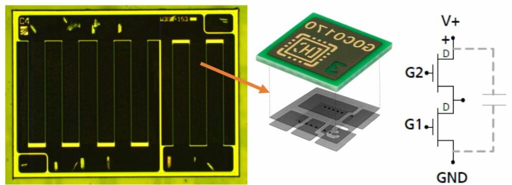
Figure 6: Photography of a fabricated half-bridge switch with a size of 3 x 2 mm2, and the X-Ray photo of the GaN embedded device
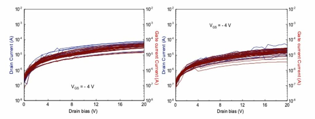
Figure 7: Breakdown voltage mapping across the 4” GaN/Si substrate for Left the low side switch, Right: for the high side switch
For testing the robustness of the embedded chips, (the GaN fabricated devices + the embedding technology). RECOM and AT&S performed two types of environmental tests on the embedded GaN half-bridge chips, first –a high temperature high humidity test of 96 hours at 85°C, 85%RH (HTH) and then a temperature cycling, of 2000 cycles, -55°C to +125°C (TCy). After the HTH testing, the embedded GaN chips did not see any electrical or packaging degradation. These test results show that AT&S’ embedding technology successfully packaged the monolithically half-bridge converters. The performance of the embedded chips did not degrade due to this technology and, as expected, a decrease into the on-resistance of each single switch was achieved.
Magnetics-on-Silicon (MoS) Micro-Transformers
At Tyndall, a magnetics-on-silicon micro-transformer (MoS-GD-Tx) for use as a gate drive isolator for a high frequency (10 – 30 MHz) LLC resonant converter was designed, fabricated and characterized[1]. The construction of the solenoidal device is as shown, using electroplated Cu and multiple laminations of sputtered CoZrTaB metal alloy layers, interspersed with AlN dielectric layers. The total device thickness is ~ 40 µm.
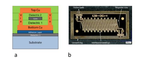
Figure 8: Schematic cross-section of MoS solenoid transformer, b) completed transformer device
Electrical characterization demonstrated that the transformers are capable of operating at any frequency in the range 20 MHz to 100 MHz. These could ultimately be a part of chip-scale heterogeneously integrated gate driver and switch.
PCB embedded inductors – Tyndall, AT&S and RECOM
A large variety of PCB embedded inductors targeted for use with GaN HEMTs in Point-of-Load (POL or iVR) DC-DC converter applications such as for 12:1 V, 2-level buck converter at multi-MHz were designed, fabricated and characterized[2]. Magnetic materials, analyses and device designs were performed by Tyndall and fabricated by AT&S, using their advanced Center Core Embedding (CCE) in-PCB technology, as shown in the figure below. The PCB embedded trials used a range of identified candidate magnetic sheet materials and Tyndall’s own released sputtered CoZrTaB material. RECOM performed some magnetic device characterisations, converter designs and were responsible for all reliability trials.
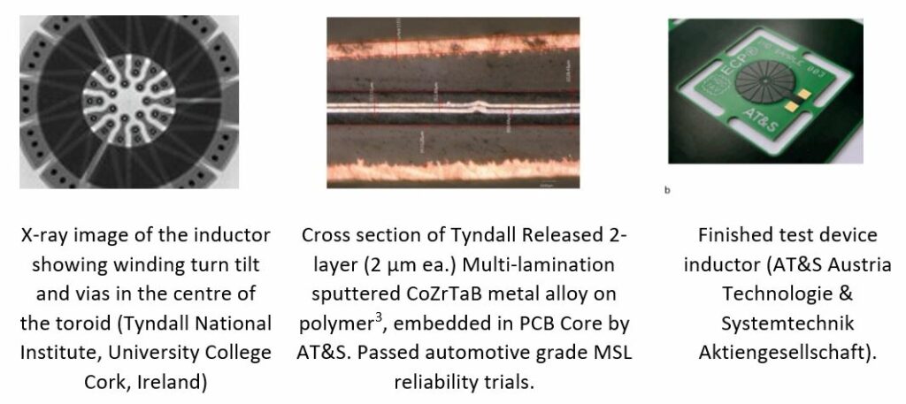
Figure 9: X-ray image, cross-section and finished PCB
[1] Zoran Pavlovic, Pranay Podder, Dermot Dobbyn, Ansar Masood, Guannan Wei, Daniel Lordan, Paul McCloskey, Cian O’Mathuna, Séamus O’Driscoll, “Thin-film magnetics-on-silicon integrated transformer for isolated power conversion applications”, CIPS 2020, Tyndall National Institute , University College Cork, Ireland.
[2] Ruaidhrí Murphya, Zoran Pavlovica, Paul McCloskeya, Cian Ó Mathúnaa, Séamus O’Driscolla, Gerald Weidingerb, “PCB Embedded Toroidal Inductor for 2MHz Point-of-Load Converter”, CIPS 2020
[3] D. Jordan et al, “High Q-Factor PCB Embedded Flip-Chip Inductors with Multi-Layer CZTB Magnetic Sheet for Power Supply in Package (PwrSiP)”, DOI 10.1109/JESTPE.2020.2983125
Our complete results brief is also available for download here.